- 您现在的位置:买卖IC网 > Sheet目录3872 > PIC18F4450T-I/ML (Microchip Technology)IC PIC MCU FLASH 8KX16 44QFN
181
XMEGA A [MANUAL]
8077I–AVR–11/2012
15.7
Register Description
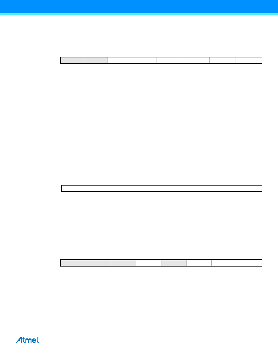
15.7.1 CTRL – Control register
Bit 7:6 – Reserved
These bits are unused and reserved for future use. For compatibility with future devices, always write these bits to zero
when this register is written.
Bit 5 – PGM: Pattern Generation Mode
Setting this bit enables the pattern generation mode as well as the CWCM mode, and disables the OUTOVEN register
action. This will override the DTI, and the pattern generation reuses the dead-time registers for storing the pattern.
Bit 4 – CWCM: Common Waveform Channel Mode
If this bit is set, the CC channel A waveform output will be used as input for all the dead-time generators. CC channel B,
C, and D waveforms will be ignored.
Bit 3:0 – DTICCxEN: Dead-Time Insertion CCx Enable
Setting these bits enables the dead-time generator for the corresponding CC channel. This will override the timer/counter
waveform outputs.
15.7.2 FDEMASK – Fault Detect Event Mask register
Bit 7:0 – FDEVMASK[7:0]: Fault Detect Event Mask
These bits enable the corresponding event channel as a fault condition input source. Events from all event channels will
be ORed together, allowing multiple sources to be used for fault detection at the same time. When a fault is detected, the
fault detect flag (FDF) is set and the fault detect action (FDACT) will be performed.
15.7.3 FDCTRL - Fault Detection Control register
Bit 7:5 – Reserved
These bits are unused and reserved for future use. For compatibility with future devices, always write these bits to zero
when this register is written.
Bit 4 – FDDBD: Fault Detection on Debug Break Detection
By default, when this bit is cleared and fault protection is enabled, and OCD break request is treated as a fault. When this
bit is set, an OCD break request will not trigger a fault condition.
Bit
7
6
5
4
3
2
1
0
+0x00
–
PGM
CWCM
DTICCDEN
DTICCCEN
DTICCBEN
DTICCAEN
Read/Write
R
R/W
Initial Value
0
Bit
7
6
5432
10
+0x02
FDEVMASK[7:0]
Read/Write
R/W
Initial Value
0
0000
00
Bit
7
6
54321
0
+0x03
–
FDDBD
–
FDMODE
FDACT[1:0]
Read/Write
R
R/W
R
R/W
Initial Value
0
00000
0
发布紧急采购,3分钟左右您将得到回复。
相关PDF资料
PIC18F4321T-I/ML
IC PIC MCU FLASH 4KX16 44QFN
PIC18F4221T-I/ML
IC PIC MCU FLASH 2KX16 44QFN
PIC18F2321T-I/ML
IC PIC MCU FLASH 4KX16 28QFN
PIC18F2221T-I/SO
IC PIC MCU FLASH 2KX16 28SOIC
PIC16LF1939-I/MV
IC MCU 8BIT 28KB FLASH 40-UQFN
PIC24F16KL402-I/SP
IC MCU 16BIT 16KB FLASH 28-SPDIP
PIC18F24J11-I/SS
IC PIC MCU FLASH 16K 2V 28-SSOP
PIC24F16KA101-I/SO
IC PIC MCU FLASH 16K 20-SOIC
相关代理商/技术参数
PIC18F4450T-I/PT
功能描述:8位微控制器 -MCU 16KB FL 768 RAM 34 I/O FS-USB 2.0 RoHS:否 制造商:Silicon Labs 核心:8051 处理器系列:C8051F39x 数据总线宽度:8 bit 最大时钟频率:50 MHz 程序存储器大小:16 KB 数据 RAM 大小:1 KB 片上 ADC:Yes 工作电源电压:1.8 V to 3.6 V 工作温度范围:- 40 C to + 105 C 封装 / 箱体:QFN-20 安装风格:SMD/SMT
PIC18F4455-BL
制造商:POWERLITE SYSTEMS 功能描述:PIC18F445 W/ BOOTLOADER FOR FLASHLAB 制造商:POWERLITE SYSTEMS 功能描述:PIC18F445 W/ BOOTLOADER, FOR FLASHLAB 制造商:POWERLITE SYSTEMS 功能描述:PIC18F445 W/ BOOTLOADER, FOR FLASHLAB; Silicon Manufacturer:Powerlite Systems; Core Architecture:PIC; Kit Contents:Board; Features:Bootloader Programming, RS232 Connector for Boot-Loading and Serial Comms ;RoHS Compliant: Yes
PIC18F4455-I/ML
功能描述:8位微控制器 -MCU 24kBF 2048RM FSUSB2 RoHS:否 制造商:Silicon Labs 核心:8051 处理器系列:C8051F39x 数据总线宽度:8 bit 最大时钟频率:50 MHz 程序存储器大小:16 KB 数据 RAM 大小:1 KB 片上 ADC:Yes 工作电源电压:1.8 V to 3.6 V 工作温度范围:- 40 C to + 105 C 封装 / 箱体:QFN-20 安装风格:SMD/SMT
PIC18F4455-I/P
功能描述:8位微控制器 -MCU 24kBF 2048RM FSUSB2 RoHS:否 制造商:Silicon Labs 核心:8051 处理器系列:C8051F39x 数据总线宽度:8 bit 最大时钟频率:50 MHz 程序存储器大小:16 KB 数据 RAM 大小:1 KB 片上 ADC:Yes 工作电源电压:1.8 V to 3.6 V 工作温度范围:- 40 C to + 105 C 封装 / 箱体:QFN-20 安装风格:SMD/SMT
PIC18F4455-I/PT
功能描述:8位微控制器 -MCU 24kBF 2048RM FSUSB2 RoHS:否 制造商:Silicon Labs 核心:8051 处理器系列:C8051F39x 数据总线宽度:8 bit 最大时钟频率:50 MHz 程序存储器大小:16 KB 数据 RAM 大小:1 KB 片上 ADC:Yes 工作电源电压:1.8 V to 3.6 V 工作温度范围:- 40 C to + 105 C 封装 / 箱体:QFN-20 安装风格:SMD/SMT
PIC18F4455T-I/ML
功能描述:8位微控制器 -MCU 24kBF 2048RM FSUSB2 RoHS:否 制造商:Silicon Labs 核心:8051 处理器系列:C8051F39x 数据总线宽度:8 bit 最大时钟频率:50 MHz 程序存储器大小:16 KB 数据 RAM 大小:1 KB 片上 ADC:Yes 工作电源电压:1.8 V to 3.6 V 工作温度范围:- 40 C to + 105 C 封装 / 箱体:QFN-20 安装风格:SMD/SMT
PIC18F4455T-I/PT
功能描述:8位微控制器 -MCU 24kBF 2048RM FSUSB2 RoHS:否 制造商:Silicon Labs 核心:8051 处理器系列:C8051F39x 数据总线宽度:8 bit 最大时钟频率:50 MHz 程序存储器大小:16 KB 数据 RAM 大小:1 KB 片上 ADC:Yes 工作电源电压:1.8 V to 3.6 V 工作温度范围:- 40 C to + 105 C 封装 / 箱体:QFN-20 安装风格:SMD/SMT
PIC18F4458-I/ML
功能描述:8位微控制器 -MCU 24KB Flash 2KB RAM RoHS:否 制造商:Silicon Labs 核心:8051 处理器系列:C8051F39x 数据总线宽度:8 bit 最大时钟频率:50 MHz 程序存储器大小:16 KB 数据 RAM 大小:1 KB 片上 ADC:Yes 工作电源电压:1.8 V to 3.6 V 工作温度范围:- 40 C to + 105 C 封装 / 箱体:QFN-20 安装风格:SMD/SMT